PCB Specifications
|
Features
|
Capability
|
Notes
|
Patterns
|
|---|
|
Layer count
|
1-20 Layers
|
The number of copper layers in the board.
|
|
|
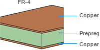
Material
|
FR-4 Aluminum Copper core Rogers / PTFE Teflon |
FR-4: Tg 135 / Tg140 / Tg155 / Tg170 Aluminum thermal conductivity: 1W/m.K Copper core thermal conductivity: 380W/m.K |
 |
|
Dielectric constant
|
4.5(double-sided PCB)
|
7628 Prepreg 4.4 3313 Perpreg 4.1 2216 Perpreg 4.16 |
|
|
Max. Dimension
|
400x500mm
|
The maximum dimension GEEKPCB can accept
|
 |
|
Dimension Tolerance
|
±0.1mm
|
±0.1mm(Precision) and ±0.2mm(Regular) for CNC routing, and ±0.4mm for V-scoring
|
|
|
Board Thickness
|
0.4 - 2.5 mm
|
Thickness for FR4 are: 0.4/0.6/0.8/1.0/1.2/2.0 mm (2.5 mm only available with 12 layers or more. )
|
 |
|
Thickness Tolerance ( Thickness≥1.0mm) |
± 10%
|
e.g. For the 1.6mm board thickness, the finished board thickness ranges from 1.44mm(T-1.6×10%) to 1.76mm(T+1.6×10%)
|
|
|
Thickness Tolerance ( Thickness<1.0mm) |
± 0.1mm
|
e.g. For the 0.8mm board thickness, the finished board thickness ranges from 0.7mm(T-0.1) to 0.9mm(T+0.1).
|
|
|
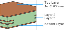
Finished Outer Layer Copper
|
1 oz / 2 oz (35um / 70um)
|
Finished copper weight of outer layer is 1oz or 2oz.
|
 |
|
Finished Inner Layer Copper
|
0.5 oz / 1 oz / 2 oz (17.5um / 35um / 70um)
|
Finished copper weight of inner layer is 0.5oz by default.
|
 |
|
Surface Finish
|
HASL (leaded / lead-free), ENIG, OSP (copper core boards only)
|
FR4 has all three finishes available, 6+ layers and RF boards only have ENIG. Aluminium core boards only have HASL. Copper core boards only have OSP. |
Drill/Hole Size
|
Features
|
Capability
|
Notes
|
Patterns
|
|---|
|
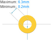
Drill Hole Size
|
0.15mm - 6.30mm
|
1 & 2 Layer PCB: 0.3 - 6.3mm Multi-Layer PCB: 0.15 - 6.3mm (0.15mm more costly) |
 |
|
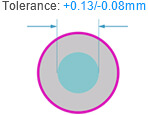
Drill Hole Size Tolerance
|
+0.13/-0.08mm
|
e.g. for the 0.6mm hole size, the finished hole size between 0.52mm to 0.73mm is acceptable.
|
|
|
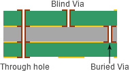
Blind/Buried Vias
|
Don’t support
|
Currently we don't support Blind/Buried Vias, only make through holes.
|
 |
|
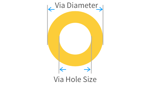
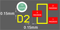
Min. Via hole size/diameter
|
0.15mm / 0.25mm
|
- 1 & 2 Layer PCB: 0.3mm(hole size) / 0.5mm(diameter) - Multi-Layer PCB: 0.15mm(Via hole size) / 0.25mm(Via diameter) ① Via diameter should be 0.1mm(0.15mm preferred) larger than Via hole size ② Preferred Min. Via hole size: 0.2mm |
 |
|
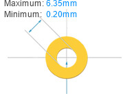
PTH hole Size
|
0.20mm - 6.35mm
|
The annular ring size will be enlarged to 0.15mm in production.
|
 |
|
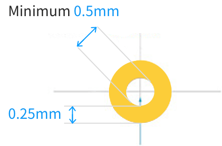
Pad Size
|
Minimum 1.0mm
|
The pad size will be enlarged by 0.5mm than the hole size. The minimum size of annular ring around plated through hole pads is 0.25mm. If the recommended sizes are not respected then the pad will not be produced properly.
|
 |
|
Min. Non-plated holes
|
0.50mm
|
The minimum NPTH dimension is 0.50mm, Please add the NPTH in the mechanical layer or keep out layer.
|
 |
|
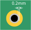
NPTH
|
0.2mm
|
We make NPTH via dry sealing film process, if customer would like a NPTH but around with pad/copper, our engineer will dig out around pad/copper about 0.2mm-0.25mm, otherwise the metal potion will be flowed into the hole and it becomes a PTH. (there will be no copper dig out optimization for single board).
|
 |
|
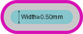
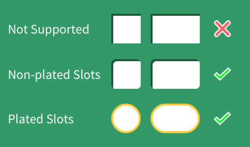
Min. Plated Slots
|
0.5mm
|
The minimum plated slot width is 0.5mm, which is drawn with a pad.
|
 |
|
Min. Non-Plated Slots
|
1.0mm
|
The minimum Non-Plated Slot Width is 1.0mm, please draw the slot outline in the mechanical layer(GML or GKO)
|
 |
|
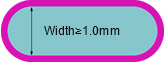
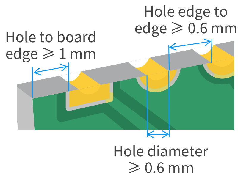
Min. Castellated Holes
|
0.60mm
|
A castellated pad includes a plated half-hole on the edge of a board, usually used on daughter PCB modules to solder to carrier boards. ① Hole diameter ≥ 0.6 mm ② Hole to board edge ≥ 1 mm ③ Min. board size 10 × 10 mm |
 |
|
Hole size Tolerance (Plated)
|
+0.13mm/-0.08mm
|
e.g. for the 1.00mm Plated hole, the finished hole size between 0.92mm to 1.13mm is acceptable.
|
 |
|
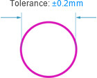
Hole size Tolerance (Non-Plated)
|
±0.2mm
|
e.g. for the 1.00mm Non-Plated hole, the finished hole size between 0.80mm to 1.20mm is acceptable.
|
 |
|
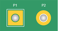
Rectangle Hole/Slot
|
Don’t support
|
Rectangle/Square Slots, we don't make rectangular or square plated holes,only make oval or round plated slots. For non-plated slots, rounded corner-rectangular or square slots are supported. The recommended minimum size is 3x3mm. |
 |
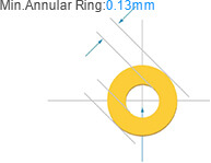
Minimum Annular Ring
|
Minimum annular ring
|
PTH
|
Patterns
|
|---|
|
1oz Copper
|
0.13mm
|
0.3mm
|
 |
|
2oz Copper
|
0.2mm
|
0.3mm
|
Minimum clearance
|
Features
|
Capability
|
Patterns
|
|---|
|
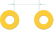
Hole to hole clearance(Different nets)
|
0.5mm
|
 |
|
Via to Via clearance(Same nets)
|
0.254mm
|
|
|
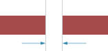
Pad to Pad clearance(Pad without hole, Different nets)
|
0.127mm
|
 |
|
Pad to Pad clearance(Pad with hole, Different nets)
|
0.5mm
|
|
|
Via to Track
|
0.254mm
|
 |
|
PTH to Track
|
0.33mm
|
|
|
NPTH to Track
|
0.254mm
|
|
|
Pad to Track
|
0.2mm
|
 |
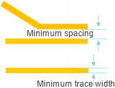
Minimum trace width and spacing
|
Min. Trace width
|
Min. Spacing
|
Patterns
|
|---|
|
1-2 Layers
|
5mil (0.127mm)
|
5mil (0.127mm)
|
 |
|
4-6 Layers
|
3.5mil (0.09mm)
|
3.5mil (0.09mm)
|
|
|
2oz Copper weight
|
8mil (0.2mm)
|
8mil (0.2mm)
|
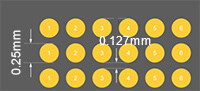
BGA
|
Layer count
|
Min. BGA Pad Dimensions
|
Min. Distance Between BGA
|
Patterns
|
|---|
|
1/2 layers
|
0.25 mm
|
0.127mm
|
 |
|
4/6 layers
|
0.25 mm
|
0.127mm
|
Solder Mask
|
Features
|
Capability
|
Notes
|
Patterns
|
|---|
|
Soldermask Expansion
|
0.038mm
|
2 layer: Expansion ≥ 0.038 mm each side; Edge of opening to adjacent traces ≥ 0.05 mm. Multilayer: No expansion required |
 |
|
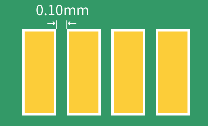
Min. Solder bridge
|
0.10mm |
2 layers: 0.10 mm regular, 0.08 mm minimum (0.13 mm with black or white soldermask). Multilayer: 0.08 mm (0.13 mm with black or white soldermask). Soldermask webs are possible between pads at least 4 mil apart. |
 |
|
Via Covering
|
Epoxy Filled & Capped Copper paste Filled&Capped |
Via hole size: 0.2 to 0.5 mm Annular ring: 0.05 mm minimum, 0.075 mm preferred The via-in-pad must be placed more than 1.0 mm from regular PTHs or NPTHs |
 |
|
Solder mask color
|
green, red, yellow, blue, white, and black.
|
We use LPI (Liquid Photo Imageable) solder mask. It is the most common type of mask used today.
|
|
|
Solder mask dielectric constant
|
3.8
|
|
|
|
Solder mask ink thickness
|
10-15UM
|
|
Legend
|
Features
|
Capability
|
Notes
|
Patterns
|
|---|
|
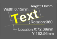
Minimum Line Width
|
6 mil (0.153mm)
|
Characters width less than 6mil(0.153mm) will be unidentifiable.
|
 |
|
Minimum text height
|
40 mil (1.0mm)
|
Characters height less than 40 mil(1.0mm) will be unidentifiable.
|
 |
|
Character width to height ratio
|
1:6
|
The preferred ratio of width to height is 1:6.
|
 |
|
Hollow-carved Character width to height ratio
|
1:6
|
The preferred ratio of width to height is 1:6
|
|
|
Pad To Silkscreen
|
0.15mm
|
The Minimum Distance Between Pad and Silkscreen is 0.15mm.
|
 |
Board Outlines
|
Features
|
Capability
|
Notes
|
Patterns
|
|---|
|
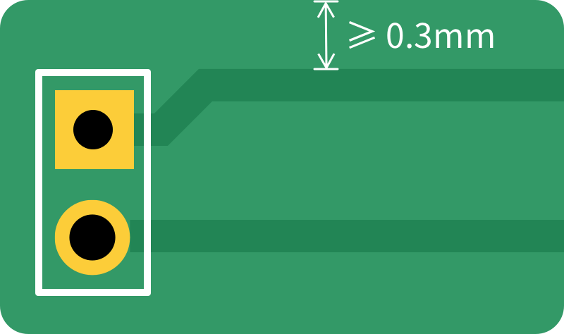
Trace to Outline(Routed)
|
0.3 mm
|
① Copper to board edge ≥ 0.3 mm ② Copper to milled slot ≥ 0.3 mm ③ Routed outline tolerance: ± 0.2 mm (regular), ± 0.1 mm (precision) |
 |
|
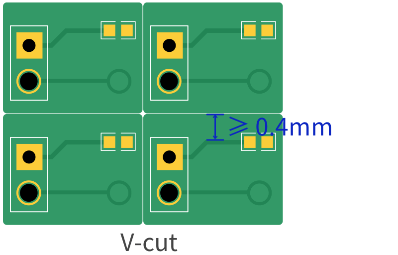
Trace to V-cut line(V-Cut Panel)
|
0.4 mm
|
① Copper to V-cut line ≥ 0.4 mm ② V-cut outline tolerance ± 0.4 mm (board thickness ≥ 0.6 mm) ③ Zero spacing between sub-boards by default. If using V-cuts on two opposing edges only, 1.6 or 2.0 mm spacing can be used on the other edges. |
 |
|
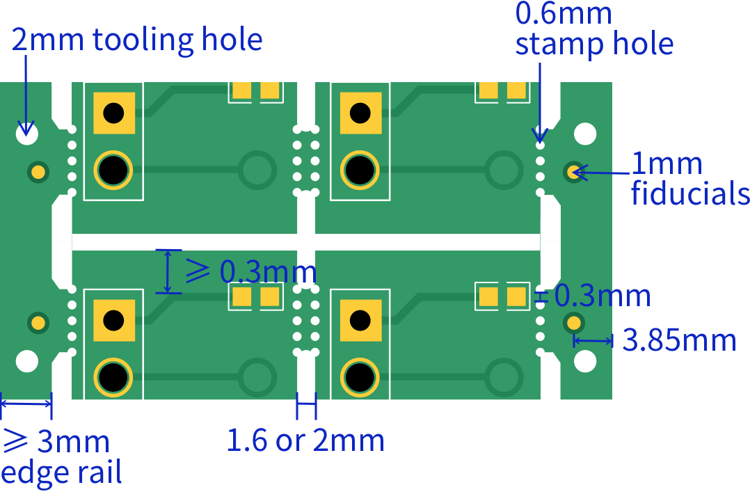
Mouse Bites Panel
|
0.3 mm
|
① Copper to routed parts of edges ≥ 0.3 mm ② Routed outline tolerance: ± 0.2 mm (regular), ± 0.1 mm (precision) ③ 1.6 or 2.0mm spacing between sub-boards by default. ④ Stamp-like edges will remain after separation ⑤ Minimum edge rail is 3mm in width. For PCB assembly, use 5mm edge rails, 1mm fiducials placed, 2mm tooling holes, 3.85mm from fiducial to board edge. |
 |
Panelization
|
Features
|
Capability
|
Notes
|
Patterns
|
|---|
|
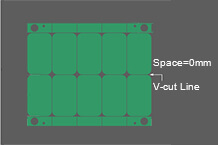
Panelization without space
|
0mm
|
The space between boards is 0mm.
|
 |
|
Panelization with space
|
2mm
|
Make sure the space between boards should be ≥2mm,otherwise it will be hard to process for rounding.
|
 |
|
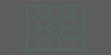
Panelized Round board
|
≥20mmx20mm
|
The single round board size should be≥20mmx20mm. Panelize with stamp holes and add tooling strips on four board edges |
 |
|
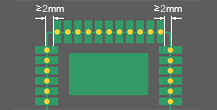
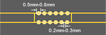
Panelized castellated holes board
|
Panelize with stamp holes and add tooling strips on four board edges
|
The distance between castellated hole and board corner should be larger than 2mm. Recommended diameter of stamp hole is 0.5mm-0.8mm; Recommended distance between the two stamp holes is 0.2-0.3mm |
|
|
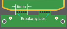
Min. Width of Breakaway Tab
|
4mm
|
The minimum width of breakaway tab is 4mm. For breakaway with mouse-bites, the minimum width is 5mm.
|
 |
|
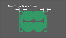
Min. Edge Rails
|
3mm
|
If choosing panel by GEEKPCB, we will add 5mm edge rails on both sides by default.
|
 |